- 您现在的位置:买卖IC网 > Sheet目录342 > MC34845BEPR2 (Freescale Semiconductor)IC LED DVR BACKLIGHT 6CH 24QFN
�� �
�
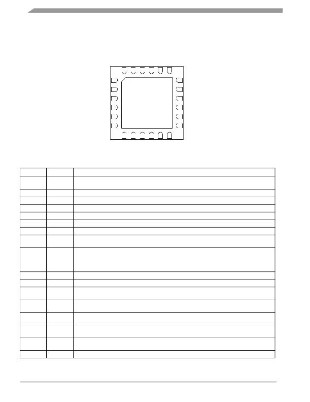
�PIN� CONNECTIONS�
�STATIC� AND� DYNAMIC� ELECTRICAL� CHARACTERISTICS�
�PIN� CONNECTIONS�
�TRANSPARENT�
�TOP� VIEW�
�24�
�23�
�22�
�21�
�20�
�19�
�VIN�
�PGNDB�
�SWB�
�SWA�
�PGNDA�
�EN�
�1�
�2�
�3�
�4�
�5�
�6�
�EP� GND�
�18� WAKE�
�17� COMP�
�16� PWM�
�15� ISET�
�14� FAIL�
�13� GND�
�7�
�8�
�9�
�10�
�11�
�12�
�Figure� 3.� 34845� Pin� Connections�
�Table� 4.� 34845� Pin� Definitions�
�Pin� Number�
�1�
�2�
�3�
�4�
�5�
�6�
�7� -� 12�
�13,� 19,� 21�
�14�
�15�
�16�
�17�
�18�
�20�
�22�
�23�
�24�
�Pin� Name�
�VIN�
�PGNDB�
�SWB�
�SWA�
�PGNDA�
�EN�
�CH1� -� CH6�
�GND�
�FAIL�
�ISET�
�PWM�
�COMP�
�WAKE�
�VDC1�
�OVP�
�VDC2�
�VOUT�
�Definition�
�Main� voltage� supply� Input.� IC� Power� input� supply� voltage,� is� used� internally� to� produce� internal� voltage� regulation�
�for� logic� functioning,� and� also� as� an� input� voltage� for� the� boost� regulator.�
�Power� ground.� This� is� the� ground� terminal� for� the� internal� Boost� FET.�
�Boost� switch� node� connection� B.� Switching� node� of� boost� converter.�
�Boost� switch� node� connection� A.� Switching� node� of� boost� converter.�
�Power� ground.� This� is� the� ground� terminal� for� the� internal� Boost� FET.�
�Enable� pin� (active� high,� internal� pull-down).�
�LED� string� connections� 1� to� 6.� LED� current� drivers.� Each� line� has� the� capability� of� driving� up� to� 30� mA.�
�Ground� Reference� for� all� internal� circuits� other� than� the� Boost� FET.� The� Exposed� Pad� (EP)� should� be� used� for�
�thermal� heat� dissipation.�
�Fault� detected� pin� (open� drain):�
�No� Failure� =� Low-impedance� pull-down�
�Failure� =� High-impedance�
�When� a� fault� situation� is� detected,� this� pin� goes� into� high� impedance.�
�LED� current� setting.� The� maximum� current� is� set� using� a� resistor� from� this� pin� to� GND.�
�External� PWM� control� signal.�
�Boost� compensation� component� connection.� This� passive� terminal� is� used� to� compensate� the� boost� converter.�
�Add� a� capacitor� and� a� resistor� in� series� to� GND� to� stabilize� the� system� as� well� as� a� shunt� capacitor.�
�Low� power� consumption� mode� for� single� wire� control.� This� is� achieved� by� connecting� the� WAKE� and� PWM� pins�
�together� and� grounding� the� ENABLE� (EN)� pin.�
�2.5� V� internal� voltage� decoupling.� This� pin� is� for� internal� use� only,� and� not� to� be� used� for� other� purposes.� A�
�capacitor� of� 2.2� μ� F� should� be� connected� between� this� pin� and� ground.�
�External� boost� over-voltage� setting.� Requires� a� resistor� divider� from� VOUT� to� GND.� If� no� external� OVP� setting�
�is� desired,� this� pin� should� be� grounded.�
�6.0� V� internal� voltage� decoupling.� This� pin� is� for� internal� use� only,� and� not� to� be� used� for� other� purposes.� A�
�capacitor� of� 2.2� μ� F� should� be� connected� between� this� pin� and� ground.�
�Boost� voltage� output� feedback.�
�34845�
�Analog� Integrated� Circuit� Device� Data�
�10�
�Freescale� Semiconductor�
�发布紧急采购,3分钟左右您将得到回复。
相关PDF资料
MC34848EPR2
IC LED DVR BACKLIGHT 8CH 48QFN
MC56F8006DEMO-T
BOARD DEMO FOR MC56F8006 DSP
MCB1114
BOARD EVALUATION FOR NXP LPC1114
MCB11C14
BOARD EVAL FOR NXP LPC11C14
MCB2470
BOARD EVAL NXP LPC247X SERIES
MCBSTM32EXL
BOARD EVALUATION FOR STM32F103ZE
MCBTMPM330
BOARD EVAL TOSHIBA TMPM330 SER
MCIMX25WPDKJ
KIT DEVELOPMENT WINCE IMX25
相关代理商/技术参数
MC34845CEP
功能描述:LED照明驱动器 6-Ch LED Backlt Driver RoHS:否 制造商:STMicroelectronics 输入电压:11.5 V to 23 V 工作频率: 最大电源电流:1.7 mA 输出电流: 最大工作温度: 安装风格:SMD/SMT 封装 / 箱体:SO-16N
MC34845CEPR2
功能描述:LED照明驱动器 6-Ch LED Backlt Driver RoHS:否 制造商:STMicroelectronics 输入电压:11.5 V to 23 V 工作频率: 最大电源电流:1.7 mA 输出电流: 最大工作温度: 安装风格:SMD/SMT 封装 / 箱体:SO-16N
MC34845DEP
功能描述:LED照明驱动器 6-Ch LED Backlt Driver RoHS:否 制造商:STMicroelectronics 输入电压:11.5 V to 23 V 工作频率: 最大电源电流:1.7 mA 输出电流: 最大工作温度: 安装风格:SMD/SMT 封装 / 箱体:SO-16N
MC34845DEPR2
功能描述:LED照明驱动器 6-Ch LED Backlt Driver RoHS:否 制造商:STMicroelectronics 输入电压:11.5 V to 23 V 工作频率: 最大电源电流:1.7 mA 输出电流: 最大工作温度: 安装风格:SMD/SMT 封装 / 箱体:SO-16N
MC34845EP
功能描述:LED照明驱动器 6-Ch LED Backlt Driver RoHS:否 制造商:STMicroelectronics 输入电压:11.5 V to 23 V 工作频率: 最大电源电流:1.7 mA 输出电流: 最大工作温度: 安装风格:SMD/SMT 封装 / 箱体:SO-16N
MC34845EPR2
功能描述:LED照明驱动器 6-Ch LED Backlt Driver RoHS:否 制造商:STMicroelectronics 输入电压:11.5 V to 23 V 工作频率: 最大电源电流:1.7 mA 输出电流: 最大工作温度: 安装风格:SMD/SMT 封装 / 箱体:SO-16N
MC34846EP
功能描述:LED照明驱动器 6-Ch LED Backlt Drvr RoHS:否 制造商:STMicroelectronics 输入电压:11.5 V to 23 V 工作频率: 最大电源电流:1.7 mA 输出电流: 最大工作温度: 安装风格:SMD/SMT 封装 / 箱体:SO-16N
MC34846EPR2
功能描述:LED照明驱动器 6-Ch LED Backlt Drvr RoHS:否 制造商:STMicroelectronics 输入电压:11.5 V to 23 V 工作频率: 最大电源电流:1.7 mA 输出电流: 最大工作温度: 安装风格:SMD/SMT 封装 / 箱体:SO-16N